Click

Saturday, March 1, 2014

Low Level Graphics API Developments @ GDC 2014?

With the annual Game Developer Conference taking place next month in San Francisco, the session catalogs for the conference are finally being published and it looks like we may be in for some interesting news on the API front. Word comes via the Tech Report and regular contributor SH SOTN that 3 different low level API sessions have popped up in the session catalog thus far. These sessions are covering both Direct3D and OpenGL, and feature the 4 major contributors for PC graphics APIs: Microsoft, AMD, NVIDIA, and Intel.
The session descriptions only offer a limited amount of information on their respective contents, so we don’t know whether anything here is a hard product announcement or whether it’s being presented for software research & development purposes, but at a minimum it would give us an idea into what both Microsoft and the OpenGL hardware members are looking into as far as API efficiency is concerned. The subject has become an item of significant interest over the past couple of years, first with AMD’s general clamoring for low level APIs, and more recently with the launch of their Mantle API. And with the console space now generally aligned with the PC space (x86 CPUs + D3D11 GPUs), now is apparently as good a time as any to put together a low level API that can reach into the PC space.
With GDC taking place next month we’ll know soon enough just what Microsoft and its hardware partners are planning. In the meantime let’s take a quick look at the 3 sessions.

DirectX: Evolving Microsoft's Graphics Platform

Presented by: Microsoft; Anuj Gosalia, Development Manager, Windows Graphics
For nearly 20 years, DirectX has been the platform used by game developers to create the fastest, most visually impressive games on the planet.
However, you asked us to do more. You asked us to bring you even closer to the metal and to do so on an unparalleled assortment of hardware. You also asked us for better tools so that you can squeeze every last drop of performance out of your PC, tablet, phone and console.
Come learn our plans to deliver.

Direct3D Futures

Presented by: Microsoft; Max McMullen, Development Lead, Windows Graphics
Come learn how future changes to Direct3D will enable next generation games to run faster than ever before!
In this session we will discuss future improvements in Direct3D that will allow developers an unprecedented level of hardware control and reduced CPU rendering overhead across a broad ecosystem of hardware.
If you use cutting-edge 3D graphics in your games, middleware, or engines and want to efficiently build rich and immersive visuals, you don't want to miss this talk.

Approaching Zero Driver Overhead in OpenGL

Presented By: NVIDIA; Cass Everitt, OpenGL Engineer, NVIDIA; Tim Foley, Advanced Rendering Technology Team Lead, Intel; John McDonald,  Senior Software Engineer, NVIDIA; Graham Sellers,  Senior Manager and Software Architect, AMD
Driver overhead has been a frustrating reality for game developers for the entire life of the PC game industry. On desktop systems, driver overhead can decrease frame rate, while on mobile devices driver overhead is more insidious--robbing both battery life and frame rate. In this unprecedented sponsored session, Graham Sellers (AMD), Tim Foley (Intel), Cass Everitt (NVIDIA) and John McDonald (NVIDIA) will present high-level concepts available in today's OpenGL implementations that radically reduce driver overhead--by up to 10x or more. The techniques presented will apply to all major vendors and are suitable for use across multiple platforms. Additionally, they will demonstrate practical demos of the techniques in action in an extensible, open source comparison framework.

NVIDIA's Tegra Note 7 LTE and Tegra 4i Devices: Hands On

Yesterday I spent some time with NVIDIA where I played with the newly announced Tegra Note 7 LTE. Internally the $299 Note 7 LTE is identical to the WiFi-only version, but with the inclusion of a NVIDIA i500 mini PCIe card. 
As many of you noticed in our announcement post of the Tegra Note 7 LTE, there is an increase in weight for the LTE version. It turns out the added weight is because the Note 7 LTE actually gets a slightly redesigned chassis that's a bit more structurally sound. The main visual change is on the back cover which now looks more 2013 Nexus 7-like.
The Tegra Note 7 LTE was able to connect and transact data on a live LTE network. NVIDIA tells me that devices will be available sometime in Q2 and will ship fully unlocked. NVIDIA did add that the final list of bands supported might change.
NVIDIA also had the Wiko WAX, which is one of the first (if not the first) retail Tegra 4i device. The WAX features a 4.7" 720p display, 8MP rear facing camera and obviously NVIDIA's Tegra 4i. NVIDIA expects availability in Europe beginning in April. 

Samsung's Exynos 5422 & The Ideal big.LITTLE: Exynos 5 Hexa (5260)

Samsung announced two new mobile SoCs at MWC today. The first is an update to the Exynos 5 Octa with the new Exynos 5422. The 5422 is a mild update to the 5420, which was found in some international variants of the Galaxy Note 3. The new SoC is still built on a 28nm process at Samsung, but enjoys much higher frequencies on both the Cortex A7 and A15 clusters. The two clusters can run their cores at up to 1.5GHz and 2.1GHz, respectively.
The 5422 supports HMP (Heterogeneous Multi-Processing), and Samsung LSI tells us that unlike the 5420 we may actually see this one used with HMP enabled. HMP refers to the ability for the OS to use and schedule threads on all 8 cores at the same time, putting those threads with low performance requirements on the little cores and high performance threads on the big cores.
The GPU is still the same ARM Mali-T628 MP6 from the 5420, running at the same frequency. Samsung does expect the 5422 to ship with updated software (drivers perhaps?) that will improve GPU performance over the 5420.
Exynos 5 Comparison
SoC52505260541054205422
Max Number of Active Cores2644 (?)8
CPU Configuration2 x Cortex A152 x Cortex A15 + 4 x Cortex A74 x Cortex A15 + 4 x Cortex A74 x Cortex A15 + 4 x Cortex A74 x Cortex A15 + 4 x Cortex A7
A15 Max Clock1.7 GHz1.7GHz1.6GHz1.8GHz2.1GHz
A7 Max Clock-1.3GHz1.2GHz1.3GHz1.5GHz
GPUARM Mali-T604 MP4ARM Mali-T624 (?)Imagination PowerVR SGX544MP3ARM Mali-T628 MP6ARM Mali-T628 MP6
Memory Interface2 x 32-bit LPDDR3-16002 x 32-bit LPDDR3-1600 (?)2 x 32-bit LPDDR3-16002 x 32-bit LPDDR3-18662 x 32-bit LPDDR3-1866
Process32nm HK+MG28nm HK+MG (?)28nm HK+MG28nm HK+MG28nm HK+MG 
The launch vehicle for the 5422 is likely the recently announced Galaxy S 5. Although most of what we'll encounter will ship with Qualcomm's Snapdragon 801, we'll likely see some international variants with the 5422. It's also entirely possible that some future Exynos 5422 SGS5 variants will feature an Intel XMM 7160 LTE modem.
The more exciting news however is the new Exynos 5 Hexa, a six-core big.LITTLE HMP SoC. With a design that would make Peter Greenhalgh proud, the Exynos 5260 features two ARM Cortex A15 cores running at up to 1.7GHz and four Cortex A7 cores running at up to 1.3GHz. The result is a six core design that is likely the best balance of performance and low power consumption. HMP is fully supported so a device with the proper scheduler and OS support would be able to use all 6 cores at the same time.
The 5260 feels like the ideal big.LITTLE implemention. I'm not expecting to find the 5260 in many devices, but I absolutely want to test a platform with one in it. If there was ever a real way to evaluate the impact of big.LITTLE, it's Samsung's Exynos 5260.
Samsung didn't announce cache sizes, process node or GPU IP for the 5260. Earlier leaks hinted at an ARM Mali T624 GPU. Samsung's release quotes up to 12.8GB/s of memory bandwidth, which implies a 64-bit wide LPDDR3-1600 interface.

Modular Smartphone Project Ara from Google to Start Development Conferences

Joshua talked about Project Ara (from Motorola at the time) back in October as a campaign that focused on attracting OEM interest into a modular smartphone design.  The results of that campaign take the next step forward as Google announces the first set of developer conferences for a modular device.
Headed under the Advanced Technology and Projects (ATAP) division, the platform is meant to be a single hub onto which the user can place their own hardware.  This means CPUs, cameras, sensors, screens, baseband, modems, connectivity, storage – the whole gamut.  The issue with such a device compounds the effects of going from a managed ecosystem (Apple and several hardware combinations) to a free ecosystem (Android and every hardware combination).  Project Ara takes this complexity one stage further, and there has to be a fundamental software base to solve this.  Hence ATAP is going to be doing three developers’ conferences in 2014, starting on April 15-16 at the Computer History Museum in Mountain View, California.
Aside from those attending in person, the event will be live webcast with question and answer sessions built into the programme.  Due to the early stage of Project Ara, the initial conference is all about the modular system itself, building a device and getting it to work.  Coinciding with the first conference, an alpha version of the Module Developers’ Kit should be available.
The other two conferences for 2014 are yet to be announced.  Further info on the conference is found at the website projectara.com, to be updated over the next few weeks with more details.
To quote the website:
We plan a series of three Ara Developers’ Conferences throughout 2014. The first of these, scheduled for April 15-16, will focus on the alpha release of the Ara Module Developers’ Kit (MDK). The MDK is a free and open platform specification and reference implementation that contains everything you need to develop an Ara module. We expect that the MDK will be released online in early April.
The Developers’ Conference will consist of a detailed walk-through of existing and planned features of the Ara platform, a briefing and community feedback sessions on the alpha MDK, and an announcement of a series of prize challenges for module developers. The complete Developers’ Conference agenda will be out in the next few weeks.
This first version of the MDK relies on a prototype implementation of the Ara on-device network using the MIPI UniPro protocol implemented on FPGA and running over an LVDS physical layer. Subsequent versions will soon be built around a much more efficient and higher performance ASIC implementation of UniPro, running over a capacitive M-PHY physical layer.
The Developers’ Conference, as the name suggests, is a forum targeted at developers so priority for on-site attendance will reflect this. For others--non-developers and Ara enthusiasts--we welcome you to join us via the live webstream. That said, we invite developers of all shapes and sizes: from major OEMs to innovative component suppliers to startups and new entrants into the mobile space.

Intel SSD 730 (480GB) Review: Bringing Enterprise to the Consumers

The days of Intel being the dominant player in the client SSD business are long gone. A few years ago Intel shifted its focus from the client SSDs to the more profitable and hence alluring enterprise market. As a result of the move to SandForce silicon, Intel's client SSD lineup became more generic and lost the Intel vibe of the X-25M series. While Intel still did its own thorough validation to ensure the same quality as with its fully in-house designed drives, the second generation SandForce platform didn't allow much OEM customization, which is why the SSD 520 and other SandForce based Intel SSDs turned out to be very similar to the dozens of other SandForce driven SSDs in the market.
The SSD market has matured since the X-25M days and a part of the maturing process involves giving up profits. Back in 2007-2008 the SSD market (both client and enterprise) was a niche with low volume and high profits, so it made sense for Intel to invest in custom client-oriented silicon. There wasn't much competition and given Intel's resources and know-how, they were able to build a drive that was significantly better than the other offerings.
The high profits, however, attracted many other manufacturers as well and in the next few years Intel faced a situation it didn't like: profit margins were going down, yet bigger and bigger investments had to be made in order to stay competitive in the client market. OCZ in particular was heavily undercutting Intel's pricing and big companies with technological and scale advantage like Intel tend not to like the bargain game because at the end of the day it's not as profitable for them. The enterprise market is a bit different in this regard because price is not usually the commanding factor; instead the focus is on reliability, features and performance, which made it an easy choice for Intel to concentrate its resources on covering that market instead.
For the majority of consumers this change in focus was negligible since the likes of Micron and Samsung had started paying attention to the retail consumer SSD market and Intel was no longer the only good option available. However, enthusiasts were left yearning for an Intel SATA 6Gbps design as many had built brand loyalty for Intel with the X-25M. In late 2012 the wishes materialized but to their disappointment only in the form of an enterprise SSD: the DC S3700
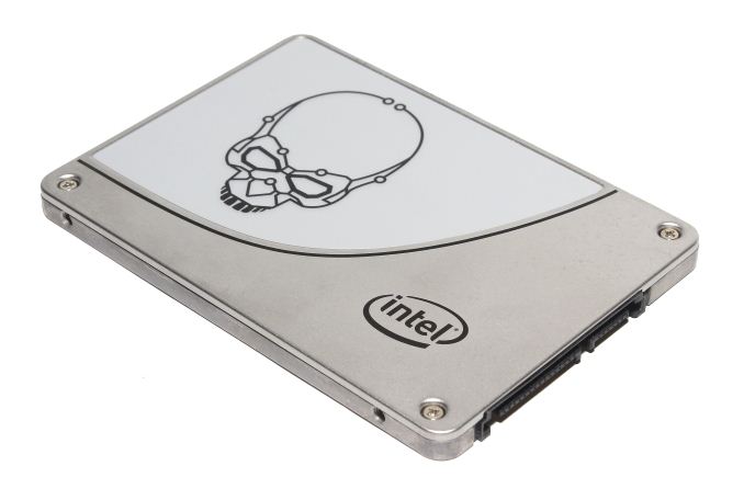
Adopting the platform from the DC S3500/S3700, the SSD 730 is Intel's first fully in-house designed client drive since the SSD 320. The SSD 730 is not just a rebranded enterprise drive, though, as both the controller and NAND interface are running at higher frequencies for increased peak performance. While the branding suggests that this is an enterprise drive like the SSD 710, Intel is marketing the SSD 730 directly to consumers and the DC S3xxx along with the 900 series remain as Intel's enterprise lineups. And in a nod to enthusiasts, the SSD 730 adopts the Skulltrail logo to further emphasize that we are dealing with some serious hardware here.
Capacity240GB480GB
ControllerIntel 3rd Generation (SATA 6Gbps)
NANDIntel 20nm MLC
Sequential Read550MB/s550MB/s
Sequential Write270MB/s470MB/s
4K Random Read86K IOPS89K IOPS
4K Random Write56K IOPS74K IO
Power (idle/load)1.5W / 3.8W1.5W / 5.5W
Endurance50GB/day (91TB total)70GB/day (128TB total)
WarrantyFive years
AvailabilityPre-orders February 27th - Shipping March 18th
Intel is serious about the SSD 730 being an enterprise-class drive for the client market as even the NAND is pulled from the same batch as Intel's MLC-HET NAND used in the S3700 and the endurance rating is based on JEDEC's enterprise workload. JEDEC's SSD spec, however, requires that client SSDs must have a data retention time of one year minimum whereas enterprise drives must be rated at only three months, which gives the S3500/S3700 a higher endurance. MLC-HET also trades performance for endurance by using lower programming voltages, resulting in less stress on the silicon oxide.
 Intel SSD 730Intel SSD 530Intel SSD DC S3500Intel SSD DC S3700
Capacities (GB)240, 48080, 120, 180, 240, 360, 48080, 120, 160, 240, 300, 400, 480, 600, 800100, 200, 400, 800
NAND20nm MLC20nm MLC20nm MLC25nm MLC-HET
Max Sequential Performance (Reads/Writes)550 / 470 MBps540 / 490 MBps500 / 450 MBps500 / 460 MBps
Max Random Performance (Reads/Writes)89K / 75K IOPS48K / 80K IOPS75K / 11.5K IOPS76K / 36K IOPS
Endurance (TBW)91TB (240GB)
128TB (480GB)
36.5TB140TB (200GB)
275TB (480GB)
3.65PB (200GB)
7.3PB (400GB)
Encryption-AES-256AES-256AES-256
Power-loss ProtectionYesNoYesYes
Continuing with the enterprise features, there is full power-loss protection similar to what's in the S3500/S3700. I'm surprised that we've seen so few client SSDs with power-loss protection. Given the recent studies of power-loss bricking SSDs, power-loss protection should make a good feature at least in the high-end SSDs.
With an enterprise platform comes its pros and cons. As the platform was originally designed for 24/7 running, there isn't any form of low-power state support. Hence even idle power consumption is a tremendous 1.5W and under load the power consumption can increase to over 5W. In fact, the SSD 730 needs so much power that it draws current from the 12V rail, which is usually only used by 3.5" hard drives. While our tests don't include temperature testing, the chassis also gets very hot and uncomfortable to touch under load. It's clear that the SSD 730 is not suited for mobile use and Intel is well aware of that. The target markets for the SSD 730 are enthusiasts and professionals who truly need the best-in-the-class IO performance.
 
Interestingly, the SSD 730 is available for pre-order from selected retailers today, which is something Intel has not done in ages. Shipments are scheduled to start on March 18th.
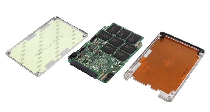
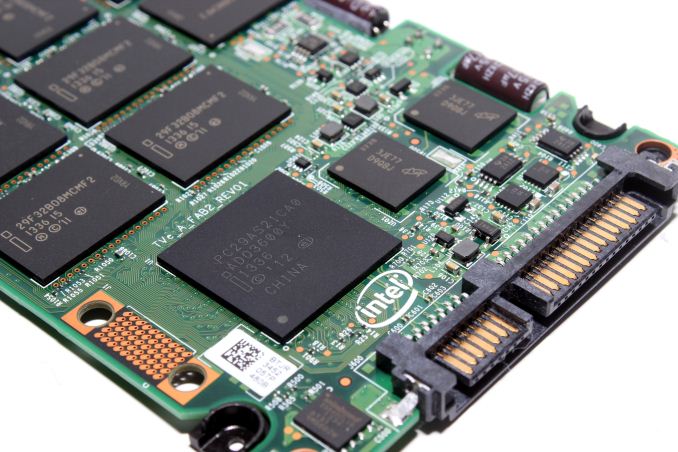
The controller is the same 8-channel design as in the S3500/S3700 but runs at 600MHz instead of the 400MHz of the S3500/S3700. It's coupled with sixteen 32GB (2x16GB) NAND packages with one of the dies designated for redundancy that protects against block and die level failures (similar to SandForce's RAISE and Micron's RAIN). This is still 64Gbit per die ONFI 2.1 NAND but compared to Intel's previous NAND, the NAND interface runs at 100MHz instead of 83MHz. As a result the bandwidth in each channel increases from 166MB/s to a maximum of 200MB/s (ONFI 2.x is a synchronous double-data-rate design), which may help in some corner cases. With an 8-channel controller the NAND interface doesn't usually play a major role because the SATA interface acts as a bottleneck and in the end we are still limited by the actual NAND performance.
 
Update: The SSD 730 actually uses 128Gbit NAND, which also expains the slow-ish write performance of the 240GB model.
 
As Intel switched to a flat indirection table design in the S3700, the SSD 730 needs way more cache than the old X-25Ms did and there are two 512MB DDR3-1600 packages to do the job. Furthermore, power-loss protection is provided by two 47 microfarad 3.5V capacitors.
 

Test System

CPUIntel Core i5-2500K running at 3.3GHz
(Turbo and EIST enabled)
MotherboardAsRock Z68 Pro3
ChipsetIntel Z68
Chipset DriversIntel 9.1.1.1015 + Intel RST 10.2
MemoryG.Skill RipjawsX DDR3-1600 4 x 8GB (9-9-9-24)
Video CardPalit GeForce GTX 770 JetStream 2GB GDDR5
(1150MHz core clock; 3505MHz GDDR5 effective)
Video DriversNVIDIA GeForce 332.21 WHQL
Desktop Resolution1920 x 1080
OSWindows 7 x64